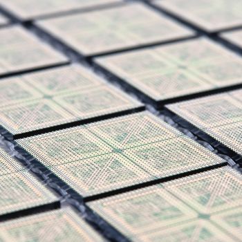
Due to growing restrictions on the use of lead in electronic products, efforts have been made to find appropriate substitutes. In the advanced IC packaging industry, the formerly ubiquitous, high-quality – but hazardous – eutectic SnPb solder bumps are now gradually being replaced by lead-free technology, such as SnAgCu alloy solder bumps. Because these new alloys require a certain composition in order to assure solderability and other mechanical properties, they must be measured precisely.
It is well known that the Ag and Cu content can exert profound impacts on the solderability and mechanical properties of Sn-based solder bumps. For instance, solder bumps with Ag content of more than 3% perform better in thermal fatigue testing and are more resistant to shear plastic deformation, while alloys with lower Ag content (around 1%) exhibit superior ductility and therefore better fatigue endurance under severe strain conditions. Furthermore, a mere 0.5% of Cu can decrease the dissolution behaviour of substrate Cu, thus increasing solderability.
That is why the IC packaging industry must accurately and precisely determine the composition of solder bumps, in order to fulfil the challenging combination of legal restrictions (being lead-free) and technical requirements.
The small size of the bumps (typically 80μm in diameter) prevents the use of most analytical methods. Others, such as atomic absorption (AA), are destructive and are therefore not suitable for testing each individual bump. However, X-ray fluorescence (XRF), has proven to be an ideal approach for monitoring the concentration of all three elements. Table 1 shows typical measurement results for a SnAgCu solder bump.
The X-ray beam of the FISCHERSCOPE® X-RAY XDV®-μ, equipped with poly-capillary optics and a silicon drift detector (SDD), can be focused down to measuring spot sizes as small as 20μm while still yielding very high count rates, guaranteeing outstanding repeatability and precision.
If accurately determining the composition of solder bumps – not only to verify lead-free technology – is important to you, the FISCHERSCOPE® X-RAY XDV-µ®, with its extremely small measuring spot, is the ideal instrument. For further information please contact your local FISCHER representative.